Tutorials in this section:
One of the basic building blocks of analog and digital circuits is the operational amplifier (or op amp), and these devices could almost be included in the same category along with transistors, resistors, and capacitors.
They can be designed into a circuit as a differentiator, integrator, summing amplifier, differential amplifier, comparator, precision diode, and many other functions. They are also commonly used as a voltage follower or level shifter, and can convert a current to a voltage, voltage to a current, etc. In short: they're very handy devices!

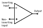
Like a transistor, an op amp is basically a three-terminal device with two high impedance differential inputs and a low impedance output. One of the two inputs is inverting and the other is non-inverting, and the difference in voltage levels on these two pins is amplified with a very high gain value which determines the voltage (or current) level on the output. In an ideal op amp, this gain would be infinite, but in real op amps, it is in the order of 20,000 to 10,000,000.
If an op amp had no feedback components connected to it, even the slightest difference in the voltage levels on the inputs (a fraction of a millivolt) could swing the output to either the full positive voltage or full negative voltage depending on which input is higher. This would be useful in comparator circuits, like those found in A/D converters.
In most op amp circuit designs, a feedback component is placed between the output pin and the inverting input pin, which creates a condition called "negative feedback". The values of the feedback component (or components) are what determine the gain characteristics, and the effect of the high open loop gain would become negligible and even cancelled out in most calculations. This is why it’s important to have the open loop gain as high as possible compared to the much lower feedback gain factor.
Besides making the external circuit behavior more predictable, using negative feedback flattens the frequency response over a larger frequency range, and allows it to be used in higher frequency applications. Negative feedback also tends to cancel out distortion and nonlinearity problems and make the circuit more temperature independent.
Positive feedback on an op amp has the feedback component connected between the output pin and the non-inverting input pin. The main purpose here is to create an oscillating circuit where the op amp output is set by the value of the feedback components and becomes independent of any input voltage applied. The finite open loop gain of op amps makes it possible for oscillations to occur.
The design specifications found in modern op amps comes so close to the ideal characteristics that designers can sometimes ignore the actual specs design the circuit based on these ideal parameters.
For an ideal op amp with perfect characteristics, it would have infinite input impedance, zero output impedance, infinite voltage gain, infinite bandwidth, zero input offset voltage, and infinite CMRR. When analyzing circuits with op amps, usually only the passive components around the circuit are considered to determine the circuit behavior. Designers would not have to worry about details like those in transistor circuit design, such as biasing and operating range.
In more critical applications, the designer would have to consider the actual specifications of the op amp.
Real op amps can have input resistances which can be in the order of a few megohms with input leakage currents from a few pico-amps to a few milli-amps. The input offset voltage is typically around a milli-volt, and the output resistance can vary from 20-1000 Ω.
The bandwidth is usually limited by something called the gain-bandwidth product (GB), which is equal to the frequency where the amplifiers gain becomes unity, usually from 1-20 MHz. The designer would need to consider phase shift limitations in the voltage gain, also.
In an ideal op amp, if both input voltages changed at precisely the same amount, it should have no effect on the output. But in real applications, there is a slight change on the output, so a designer needs to consider a parameter called the common mode rejection ratio or CMRR. The common mode voltage gain in an ideal op amp would be zero, but typically it would be about .0001. This is low enough that it could be ignored in most applications.
