EMBEDDED ADVENTURES: CONNECT THE WORLD AROUND YOU
Tutorials in this section:
The EUSART module built into the PIC18F series of microcontrollers from Microchip is an I/O communication peripheral that can be configured either in a full-duplex asynchronous mode or a half-duplex synchronous mode. This article discusses the Asynchronous mode of operation, where no clock signal is used between transmitter and receiver. This mode is typically used when communicating with external equipment, and is commonly used with RS-232, RS-485, and RS-422 systems.
As shown in the diagram, the Transmit Shift Register (TSR) is the main part of the transmitter, which shifts out the data to be transmitted to the TX/CK pin. In parallel with this is the TXREG register, which is a buffer for data to be transmitted, and a transfer of data (if any) takes place as soon as the TSR is empty.
![]()
In order to enable data transmission from a EUSART module, it is necessary to configure it to operate as a transmitter. Several bits must be set or reset for proper operation. The TXEN bit of the TXSTA register must be set to enable transmitter operation, and the SYNC bit of the TXSTA is reset to configure the EUSART for asynchronous operation. The SPEN bit of the RCSTA register must also be set to enable the EUSART and automatically configures the TX/CK I/O pin as an output.
Transmission is initiated by writing data to the TXREG register. This data will be immediately transferred over to the TSR register if it is empty. If the TSR still contains all or part of a previous character, the new character data is held in the TXREG until the Stop bit of the previous character has been transmitted. After the TXREG register is emptied, the TXIF bit of the PIR1 register is set, and this causes an interrupt if the TXIE bit of the PIE1 register is set. The TXIF bit is only clear when the TSR is busy with a character and a new character has been loaded for transmission in the TXREGx.
The transmission of the Start bit, data bits and Stop bit sequence starts immediately following the transfer of the data to the TSR from the TXREG register. As soon as the last bit leaves the TSR register, the TRMT bit of the TXSTA register is automatically set. If the TXREG register has received a new character data in the meantime, the whole procedure is repeated immediately and the TRMT is reset.
To use interrupts when transmitting data, the TXIE bit should only be set only when there is data to send and it should be cleared otherwise. When sending 9-bit data, the TX9 bit of the TXSTA register must be set and the extra bit loaded into the TX9D bit of the TXSTA register. A timing chart for transmitting one byte of data is shown:
The receiver block diagram is shown below. The data is received on the RC7/RX/DT pin and passes through the data recovery block, which is a shifting circuit operating at 16 times the baud rate, and sent to the serial Receive Shift Register (RSR), which operates at the bit rate. The data recovery block samples each data bit at a higher rate to make sure it is valid.
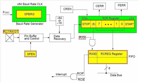
In addition to setting SYNC=0 and SPEN=1 as for the transmitter section, the receiver must be enabled by setting the CREN bit of the RCSTA register. As soon as this is done the receiver waits for a START bit, and when it is detected, data is transferred to the shift register RSR through the RX pin.
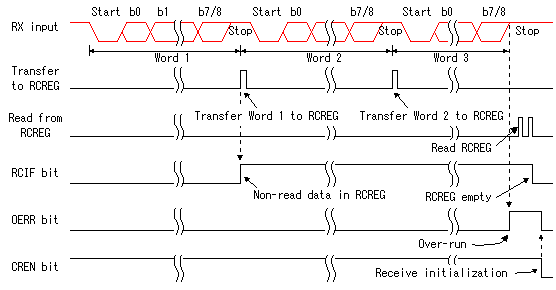
As soon as the STOP bit is received, the data is automatically transferred to the RCREG register so long as RCREG is empty. The RCREG can be checked to see if there is data ready to be read by the checking the RCIF bit of PIR1 register. The RCIF bit is automatically set when new data is available, and reading the RCREG register will automatic clear RCIF bit. If the RCIE bit of the PIE1 register is set, the RCIF bit can be used as an interrupt. To receive 9-bit data it is necessary to set the RX9 bit of the RCSTA register, and the 9th bit will then go into RX9D.
The RCREG register is set up as two First-In-First-Out (FIFO) buffers and can store two data bytes in sequence. This provides protection when the processor is delayed in reading the received data bytes. The top character is transferred out of the FIFO when reading the RCREG register. If both RCREG buffers are full and haven’t been read yet, and a third byte is being received, the OERR bit of the RCSTA register is set and an overrun error occurs. The old data which was stored in the RSR register at this time is lost. This event also clears the CREN bit and must be set again to return to normal operation. If the STOP bit fails to go to 1, this sets the FERR bit of the RCSTA register (framing error). The following timing chart shows what happens when 3 consecutive bytes are received without a read operation, causing overrun:
A test program to initialize the EUSART and perform a simple data
transmission is shown here. A 10MHz clock rate is used with the baud rate set
to 9600:
/*   Test configuration:
     MCU:             PIC18F26K22
     Dev.Board:       -
     Oscillator:      HS, 10.0000 MHz
     Ext. Modules:    -
     SW:              mikroC PRO 1.65
*/
void main(){
     char buff;
// initial USART
     SPBRG = 64;         //9600 @ 10Mhz
     TXSTA.BRGH = 1;     //High speed
     TXSTA.SYNC = 0;     //Asynchronous mode
     RCSTA.SPEN = 1;     //Serial port enable
     TXSTA.TXEN = 1;     //Transmit enable

     RCSTA.CREN = 1;     // enable reception.
     TRISC.F6 = 0;	  // configure RX and TX pins for I/O
     TRISC.F7 = 1;
     while(1){
          if (PIR1.RCIF){    // if data is ready to read
             buff = RCREG;   // store to buff
             TXREG = buff;   // send it back
             while(!TXSTA.TRMT);  //wait untill transmit compleated
          }
     }
}
In this example, the actual baud rate would be:
Baud Rate = Fosc/(16*(SPRG+1)) = 10MHz/(16*(64+1)) = 9615.38
which gives a 0.16% error.
For all modes of EUSART operation, the TRIS control bits may need to be adjusted - see the datasheet for your particular microcontroller.
This example has no error checking included. Errors for overrun error and framing error should be read from the RCSTA register bit 1 for Overrun (OERR) and bit 2 for Framing error (FERR). Both errors can be reset by clearing the SPEN bit of the RCSTA register.
The Baud Rate Generator (BRG) is a selectable 8-bit or 16-bit timer that supports both asynchronous and synchronous operation. The SPBRGHx:SPBRGx register pair determines the period of the baud rate timer. In asynchronous mode, the multiplier of the baud rate period is determined by both the BRGH bit of the TXSTA register and the BRG16 bit of the BAUDCON register. The BRGH bit selects either HIGH or LOW baud rate, and the BRG16 bit selects either 8 or 16 bits for baud the baud rate timer (SPBRGx or SPBRGHx:SPBRGx). These two bits and the SPBRG register must be set correctly for baud rate generation.
The calculation of the hexadecimal number loaded into the SPBRG register is done using the following formulas:
SPBRG = (Fosc/(16 x Baud rate)) - 1, BRGH=1 – High Speed
SPBRG = (Fosc/(64 x Baud rate)) - 1, BRGH=0 – Low Speed
Since SPBRG is rounded to the nearest whole number in this calculation, there will be slight error in the baud rate generation, as seen in the example above. It may be preferable to use the high baud rate (BRGH = 1), or the 16-bit BRG (BRG16 = 1) to reduce the baud rate error. The 16-bit BRG mode is used to achieve slow baud rates for fast oscillator frequencies.
Sometimes, especially on the receiving end, it is necessary to determine the baud rate externally. The EUSART provides an Auto-Baud Detect (ABD) mode for this, and the received data signal is used to time the BRG, rather than the BRG itself.
- James Reinholm