Page 10
27 May 12
![]()
New technologies are continually being developed to handle the crowded frequency bands over multiple channels in wireless interfaces.
Engineers tend to look for components that pack the most features in one small package, which reduces the number of total components, and enables the finished product to fit within small dimensions, like a cell phone.
Power consumption is always a major factor in these decisions, so an engineer usually chooses components that dissipate the lowest power possible with the highest level of performance. They look for enhanced parameters like increased output power, higher peak gain, and wider bandwidth in an amplifier to optimize performance and provide greater functionality.
If a device could be found that operates at more than 2 GHz of bandwidth, it could serve multiple functions on several frequency bands.

The new BGA7204 and BGA7210 from NXP Semiconductors combine this high bandwidth along with several other features and low power consumption into one small package.
These devices are both 6-bit digital variable gain amplifiers (VGAs) that feature extremely high linearity and low noise across a very wide frequency band. The BGA7210 is considered to be the only VGA of its kind capable of operating at frequencies up to 4 GHz without external matching. The BGA7204 provides 21 dBm of output power at 1 dB compression at maximum gain setting with a high output IP3 of 38 dBm. The BGA7210 delivers 23 dBm of output power with its high output IP3 of 39 dBm. Both devices offer 31.5 dB of gain control with a 6-bit 0.5 dB digital step attenuator, and have a noise figure of 6.5 dB at maximum gain. The BGA7210 provides 30 dB of maximum gain, while for the BGA7204, it is 18 dB. The BGA7210 can operate over an extremely wide bandwidth from 0.7 GHz to 3.8 GHz, while the BGA7204 is a little lower, with a bandwidth of 0.4 GHz to 2.75 GHz.
These new VGAs make sure that the incoming signal is always at optimum strength by compensating for any degradation caused by changes in temperature.
When used in wireless infrastructure equipment, the power level to the power amplifier can be controlled, which helps to compensate for variations in cell load and the presence of aging infrastructure equipment. Both products include a unique power-save mode that can reduce the current to about 15 mA, which is beneficial for Time Domain Division (TDD) systems.
The current consumption and attenuation levels are controlled through a Serial Peripheral Interface (SPI). If linearity is not critical in the application, current consumption may be reduced in the BGA7210 to 120 mA by changing the current setting. Optimal linearity performance is obtained at 185 mA. The current consumption can also be reduced in the BGA7210 according to the attenuation setting for better overall system performance. The BGA7210 can also be switched on and off based on a duty cycle, which can really save on power.
This has to be done carefully to avoid spurs that occur during the fast switching transitions.
These new VGAs would provide enhanced performance in applications like: WiMAX and cellular base stations, cable modem termination systems, temperature compensation circuits, and other IF and RF applications.
These devices come in 5 x 5 mm leadless HVQFN packages, and feature NXP’s unique smart routing lead design, which simplifies PCB placement and reduces the footprint of the device by 25 percent. Routing is simplified by the fact that the pin-outs that do not cross other connections to the package. In addition, these devices are RoHS compatible, provide ESD protection on all pins, and meet moisture sensitivity level 2.
NXP manufactures these parts by using its innovative SiGe:C QUBiC4 chip fabrication process, which allows more functionality on-chip with less space. This process has been extensively tested since 2002, and it now provides consistent parameter performance.
![]()
16 May 12
![]()
Many digital power control applications operate by using complex digital signal processing algorithms in dedicated processing devices, such as FPGA’s or DSP processors, that are designed to perform only one particular function. Microcontrollers haven’t been used in these instances because they weren’t able to continually process large amounts of data simultaneously from several input sources. Each input source would contain a digital data field that may at some specified width, such as 8, 16, or 32 bits.

These applications are usually designed to process this data at the highest possible speed and resolution while meeting certain power consumption and cost requirements.
Engineers are limited in their choice of a processing unit, as there are usually very few devices available that would perform the intended function. And once a choice is made, the device would only perform the one function it is designed for, and offers very limited flexibility.
Because of the complexity of the design, the costs almost always turn out to be much greater than the cost needed to implement a standard microcontroller into their design. The main reason for the increase in cost is that each dedicated processing unit needs specific software and other development tools that are unique to the particular device.
A general purpose MCU would have the advantage of having a standard software development tool that could be used over and over for other applications.
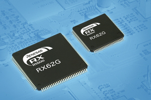
Renesas Electronics Corporation has taken a step in providing a possible solution to this problem with the new 32bit RX62G group, which is an extension of its RX600 microcontroller family.
These MCUs provide a unique combination of advanced analog features, processing power, high resolution capability and integrated timer functions. These features make the new RX62G MCUs ideal to implement high-accuracy digital control for a variety of digital power control applications, including motor control with power factor correction, power management, digital power supply, uninterrupted power supplies, and inverters/converters.
The new MCU enables complex algorithms to be implemented for processing data, along with precision control outputs at high resolution.
This can now be done at an affordable cost with standard software development tools, and enables much higher efficiency in digital power control applications. The RX62G group, which is based on high performance 32bit RX CPU core, comes with a comprehensive support ecosystem that provides a robust platform for digital power control applications. Renesas claims the RX62G group is the industry's first group of general purpose MCUs to provide this level of combined high resolution and extreme performance capability.
The new MCUs operate at 100MHz to achieve 165 Dhrystone MIPS (DMIPS) performance, and provide maximum power efficiency when operated at lower speeds while delivering high performance at higher speed. Integrated DSP functionality and floating point unit (FPU) enable efficient implementation of complex algorithms and control loops. The single-precision FPU runs separately from the RX62G CPU and simplifies decimal-point calculations, which can boost overall processing performance and simplify firmware development. With an embedded flash that works at CPU speed with no wait state, the RX62G delivers a real-time performance 165DMips at 100MHz in a pure deterministic manner.
The new series or processors feature four high-resolution timers capable of generating PWM signals with the high resolution (312.5psec) needed to control power bridges, inverters, or converters with maximum efficiency and lower power losses. When the high accuracy control is used for controlling digital power supplies in applications like servers or general power supply systems, high efficiency power management is possible.
Similar to the RX62T MCUs, the RX62G devices feature two 12-bit A/D converters and one 10-bit A/D converter unit that can capture analog input values from up to 20 channels at a minimum conversion time of 1 second. Each of the A/D converters can be triggered by timer units and can sample three phases in parallel. The RX62G MCUs also integrate a new 16-bit general-purpose pulse-width-modulation timer (GPT), and MTU3 multifunction timer-pulse units specialized for motor control. With this combination, one RX62G MCU can control up to three 3-phase motors simultaneously.
These new MCUs expand on the advanced analog and control features of the RX62T and RX63T devices, but provides enhanced performance and more efficient power consumption. The safety functions and peripheral functions of the RX62G group are upward compatible with those of the RX62T group. The safety functions enable fail-safe control for devices which use the RX62G group. The RX62G is also pin-compatible with the RX62T series, and software compatible with other members of the RX600 family. This offers better scalability options for changing design requirements for on a variety of different applications.
![]()
13 May 12
![]()
The new STC3105 battery monitor from STMicroelectronics provides the precision voltage and current measurements needed to implement a low-cost ‘gas gauge’ for portable electronic devices, such as in smart phones, tablets, and digital cameras.
Accurate predictions of the battery state-of-charge and time-to-empty can be made while monitoring the charge/discharge status of the battery. These features can extend battery life, extend operating time between charges, and help avoid unnecessary recharging. All these features are contained in a 2 x 3 x 0.8 mm package while consuming only a few micro-amps of current.
The STC3105 uses precise voltage and current measurements of the battery to estimate the battery’s state-of-charge (SOC).
A Coulomb counter is used to keep track of the state-of-charge and to track when the battery is charging or discharging. This Coulomb counter method is combined with the current and open-circuit voltage measurements to estimate the battery capacity and to supervise and track the charge/discharge status. The microcontroller can program the Coulomb counter, set the SOC base register value and read the charge register through the I2C interface. The voltage monitoring accuracy is about 0.5%, and by using an external sensing resistor, Coulomb counter accuracy is 1%.
A battery relaxation timer is used to measure the time interval that initiates when the battery charger is removed or when the current falls below a programmable load current threshold, which means the battery is in a light-load condition. The relaxation counter register is read from the I2C interface and can be checked to make sure that the battery voltage had enough time to relax from the last time the current was high or charging. The timer also indicates when an OCV (Open Circuit Voltage) measurement should be made for SOC correction.
A programmable alarm output provides a warning signal of a low State-Of-Charge (SOC) condition and/or a low battery voltage. The SOC and voltage thresholds are both programmable through the I2C interface.
The STC3105 also helps to extend the battery runtime and lifespan with several power-saving features that not only reduce its own power consumption, but the total power consumed by the application. There are two operating modes, the active mode, which draws 100 μA, and the power-saving mode, which draws 50 μA. There are also two sleep modes, the standby mode, which draws 2 μA, and the power-down mode, which draws 1 μA.
This device can initiate the necessary power-management functions when the battery is nearly empty without involving the system microcontroller, and free the microcontroller for other tasks or enable it to spend a longer time in a sleep mode. This can further increase battery life by decreasing overall power consumption, which will extend the time between charges.
![]()
12 May 2012

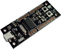
We're delighted to have the new PLT-1003 USB development platform available. Completely revised PCB, all surface mount, with more microcontroller pins broken out for your own nefarious purposes. Still with LEDs and buttons for extra control and development opportunities.

All you need to do is solder your own female or male headers as you require, and you're off and running. You can just it just as a TTL serial converter - or reprogram it to your own requirements.
In the coming weeks we'll be adding tutorials with new firmware to talk to some of our other devices, making it easier to try modules before building your own projects.
![]()
11 May 12

It's great having lots of LEDs to display graphics and text. Our LED matrix displays are a great way of doing just that. They have a simple serial interface - except that you need to update them row by row, over and over to light up the entire display.
No problems, there is code available to do that, both for Arduino and also the PicPack library.
But sometimes, you just want to display something without having to use all your precious CPU power flipping I/O pins.
Enter: the new PLT-1001 LED Matrix Display Driver board.

Cranking it up to version 4 of this board, this board gives you 16mips of processing power to keep all those LEDs flicker free.
We will be shipping it with firmware that allows you to issue simple serial commands to "Draw a circle" or "Print some text" without requiring any programming or understanding of the LED matrix displays themselves.
The other neat feature is that you can either attach a male 8x2 connector on top of the board and cable it directly to your LED Matrix Display, or solder on a female 8x2 connector under the board - and the board will attach as a "backpack" to the LED panel (for 80x8 and 64x8 boards it is the right size for the mounting holes).
Other than soldering on the connector you want to use - and terminal blocks (supplied) to connect power, the board is completely surface mount, pre-build and tested. You may need to update the firmware using a TTL serial connector for the type of LED Matrix display you wish to connect it to.
We are waiting on final PCB delivery from our manufacturing partners, and as soon as we have them available, we'll let you know. To register your interest, please email us at sales [at] embeddedadventures.com.
![]()
11 May 2012
Circuit designers usually try to use capacitors rather than inductors in their circuits because of their smaller size, reduced interference effects, and ease of manufacture. Coilcraft, Inc. has introduced a type of coil design that has made it easier to make use of coils in circuits where an inductance would work better than capacitance, such as oscillators, tuned circuits, and resonant circuits.
Coilcraft’s new PFL family of coils is especially designed for applications that require ultra-small inductors that can still handle significant current levels.

The PFL series comes in a wide assortment of footprints that would fit in a variety of applications. The new PFL4514 and PFL4517 are the latest additions to the PFL line of miniature power inductors.
These low-profile inductors feature a magnetic shield, which reduces the effects of magnetic coupling between components, and allows for tighter component spacing without electromagnetic interference. The unique PFL design provides the same performance as found in the larger standard-sized inductors, so circuit designers can now increase board density at a low cost without sacrificing any efficiency.
The PFL4514 and PFL4517 are wirewound surface-mount inductors that feature very low profiles.
The PFL4514 Series Shielded Power Inductor requires only 16 mm2 of board space and is 1.4 mm high. The 4.2 A current handling capability compares to much larger inductors. The inductance values of the PFL4514 Series range from 1.0 µH to 22 µH and feature an operating temperature range of -40 to +125°C. The DC resistance of the PFL4514 is relatively low, as low as 80 milli-ohms, making it more suitable for battery-powered devices.
The PFL4517 Series features and even lower DC resistance, which can be as low as 40 milli-ohms. Inductance values ranging from 0.68 µH to 10 µH are offered for the PFL4517. The PFL4517 is taller than the PFL4514 by 0.3 mm, and is designed for higher current levels up to 6.5A.
These low-profile, magnetically shielded inductors share a common footprint for design and prototyping flexibility. These devices have a composite-core construction with relatively heavy gauge windings to provide the high current handling capability and low DC resistance. The parts are halogen-free and RoHS-compliant, with matte tin over nickel terminations that are compatible with 260°C processing.
Coilcraft offers free evaluation samples on its website to qualifying designers, or a combined Designers Kit C451 can be purchased, which contains three samples of both the PFL4514 and PFL4517 in a range of values.
